
The big picture: TSMC is making progress on its 3nm (N3) process node plans, with N3E entering volume production later this year. The company just saw its revenue slide for the first time in four years, but it's forging ahead with significant R&D expenditures to ensure its 2nm-class nodes will be ready before Intel and others can catch up.
This week, TSMC showcased some of the key features of its current and future process node technologies at the 2023 North America Technology Symposium in Santa Clara, California. The Taiwanese company's roadmap includes a range of new silicon technologies for various industry needs that stretches to 2026, and no fewer than 1,600 partners and customers are attending the event.
Currently, TSMC is using 3nm tech (N3) in volume manufacturing – most of it for Apple silicon – and an N3E node is on schedule to start production in the second half of this year. The benefits of N3 include a speed improvement of 18 percent at the same power as N5, with logic density approaching 1.6 times that of the older node. It's also less complex (and thus less costly) to use compared to N3 since it doesn't require EUV double patterning to achieve the claimed density improvements.

Starting next year, TSMC is extending its 3nm portfolio with three new nodes: N3P, N3X, and N3AE. N3P is a refinement of N3E with the goal of further increases in transistor density while offering five percent better performance at the same power or five to ten percent more energy efficiency at the same clocks. And since it's just an optical shrink of N3E, designs based on N3P will be forward-compatible, meaning N3P will likely be a popular choice among chip design firms.
N3X is designed with high-performance computing in mind, so it will be an attractive choice for things like CPUs, GPUs, and AI accelerators. This will afford clockspeeds that are at least five percent higher compared to N3P at the cost of higher leakage currents (and thus needing higher voltages for stability). TSMC says N3X will support voltages around 1.2 volts, meaning this node will be most useful for server-grade hardware with beefy cooling systems.
TSMC plans to have N3P in mass production sometime in the second half of 2024, while N3X won't be ready until 2025. Supply chain insiders claim Intel's Celestial GPUs will be among the first to use the latter node, but we'll have to wait and see. As for N3AE, it's a node optimized for chips used in automotive applications that will also become available to carmakers in 2025.

One thing is for sure – N3 class nodes will accelerate the development of chiplet-based architectures (AMD's RDNA 3 comes to mind) with compute dies made on the latest and greatest node and additional memory and I/O dies made using more mature nodes with better cost efficiency and more predictable yields.

The company also outlined a roadmap for 2nm (N2) process nodes, which incorporate "nanosheet" (aka gate-all-around or GAAFET) transistors and allow for even better performance, energy efficiency, and increased transistor densities for logic, SRAM, and analog circuits. One advantage over existing FinFET transistors is a lower leakage current, and another is that channel width can be adjusted for either higher performance or lower power consumption.
Otherwise, TSMC claims N2 will offer 10 to 15 percent more performance at the same power as N3 or a 25 to 20 percent power reduction at the same clocks. The company is also optimistic it can achieve mixed chip densities (SRAM, logic, and analog) with N2 that are more than 15 percent higher compared to N3E.
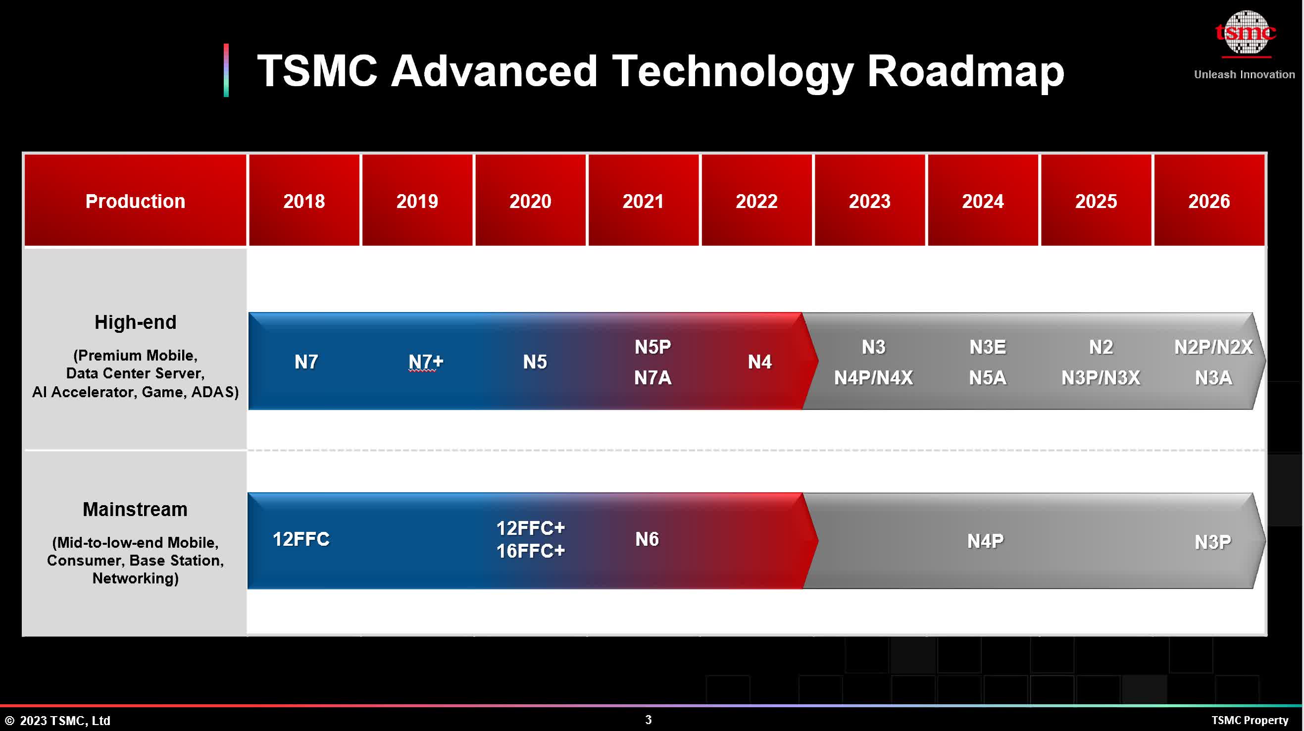
As for how far along the development process is, the new nanosheet transistors already meet 80 percent of the target performance specs, while the average yield of a 256Mb SRAM is currently hovering just above 50 percent. With high-volume production planned for 2025, the company has plenty of time to improve these figures.
The N2 family will expand sometime in 2026 with N2P, which will add backside power delivery. Just like Intel's PowerVia and Samsung's BSPDN, the idea is to sandwich the transistors between the power delivery network and the signal network, improving transistor performance and reducing power consumption as a result.

It may not sound like much, but backside power delivery networks are some of the most important innovations in the semiconductor space in recent years. It changes the way power is delivered to transistors on a chip in a way that improves power efficiency and affords significant logic density improvements. According to Applied Materials estimates, backside power delivery allows for logic cell area reductions of 20 to 30 percent – the equivalent of two lithography generations worth of improvement.
N2P won't be ready for volume manufacturing until 2026 and TSMC has yet to provide any figures on how it compares to N2. It's a similar story with N2X, the variant designed for high-performance computing where voltages and clocks are pushed to the point of diminishing returns.
If anything, Intel has a window of opportunity to catch up with TSMC with the Intel 20A and 18A nodes, with the first slated to go into volume production in late 2024. However, given Intel's poor track record of delivering on schedule and the difficulties in securing bleeding-edge ASML EUV equipment, we're not expecting any miracles.