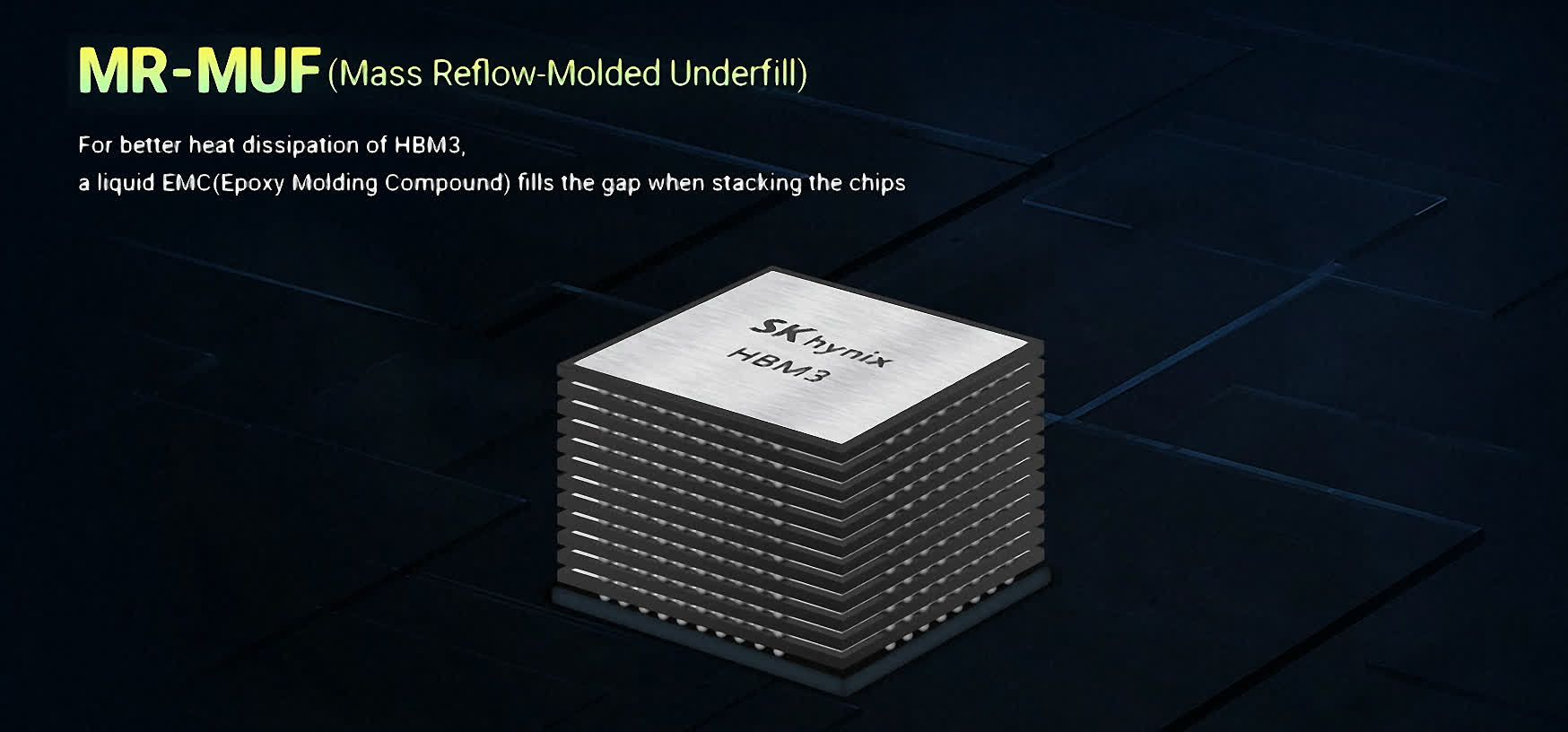
Something to look forward to: SK Hynix's newest high-bandwidth memory product, HBM3E, is currently in mass production and will be introduced into the market in the first half of this year, according to comments vice president Kim Chun-hwan made during his keynote speech at SEMICON Korea 2024 last week. By 2026 the company expects that it will be mass producing HBM4, its 6th generation HBM, he added.
Kim also provided information about the company's DRAM and NAND flash products. It is currently mass-producing 1b-level circuit line width products and developing 1c, which represents the next generation, he said. However, SK Hynix anticipates "severe technological limitations" below the 10-nanometer level and for that reason the company is pursuing the development of new materials and structures.
As generative AI gobbles up more and more capacity, the evolution of high-bandwidth memory products will be key to its continued functioning. Suppliers are rolling out second generation HBM3 products but real change will come with HBM4.
The rapid growth of generative AI is propelling demand for these memory products, with Kim noting that the generative AI market is expected to grow at an annual rate of 35%. In particular, high-bandwidth memory – first introduced to the market in 2013 amid warnings that it would never become commercially viable – allows for the lightning-fast data transfers necessary for so many of these applications.
Just to cite one example, Micron Technology boasts that its HBM3 Gen2 memory with bandwidth greater than 1.2TB/s and pin speed over 9.2Gb/s reduce training times of large language models like GPT-4. Performance, in short, has exploded.

The first iteration of high-bandwidth memory was somewhat limited, only allowing for speeds of up to 128 GB/s per stack. HBM2 doubled potential speeds to 256 GB/s per stack and maximum capacity to 8 GB.
In 2018, HBM2 received an update called HBM2E, which further increased capacity limits to 24 GB and brought another speed increase, eventually hitting 460 GB/s per chip at its peak.
The speed doubled again with the rollout of HBM3, to a maximum 819 GB/s per stack while capabilities increased to 64 GB. Then came another upgrade, HBM3E, which increased theoretical speeds up to 1.2 TB/s per stack.
Throughout this history, HBM kept the same 1024-bit per stack interface – a defining characteristic of the technology. But that will change with HBM4, expected to have a 2048-bit interface that could theoretically double transfer speeds again, assuming manufacturers are able to maintain the same transfer rates, a feat that is in doubt.
As specifications for HBM evolve, so does the market itself. Trendforce reported last year that Nvidia plans to diversify its HBM suppliers for more robust and efficient supply chain management. It also predicted a significant shift toward customization demand in the HBM4 market, moving away from the standardized approach of commodity DRAM. This move toward customization is expected to bring about unique design and pricing strategies, Trendforce said, and usher in an era of specialized production in HBM technology.
