
In context: As the technology world craves more and better performing RAM with every new manufacturing node generation, DRAM chips need to follow 3D NAND and go vertical. Lam Research is proposing some novel approaches to achieve this crucial, yet very complex (and likely expensive) goal.
Lam Research is a California-headquartered company on a mission to ignite semiconductor breakthroughs that can "define the next generation" of the technology world. One of the breakthroughs Lam is thinking about is 3D or vertically stacked DRAM memory chips, which the company estimates will evolve from traditional, 2D chips five to eight years from now "based on current technical capabilities."
Lam recently stated that the industry needs a plan to ease this crucial evolutionary step. To try and imagine this "untested future" of DRAM technology, the company used its SEMulator3D software, which is typically used to "virtually fabricate" semiconductor devices by mimicking wafer fabrication. A 3D DRAM architecture needs to address several issues with scaling, stacking, shrinking footprints, and more.
The SEMulator3D design process involved the three main components of a traditional DRAM structure, which according to Lam include a bitline to carry the electric current to be injected into a transistor. The transistor works as a gate to keep (on) or stop (off) the current traveling within the device. Lastly, a capacitor stores the aforementioned current in bit form (0 or 1).
Lam tried a few "tricks" to create a new, vertically oriented DRAM architecture by shuffling these three main components around a bit. The company's engineers tried to move the bitline over the opposite side of the transistor, which provided room for more transistors to be connected to the bitline itself with an improved chip density.
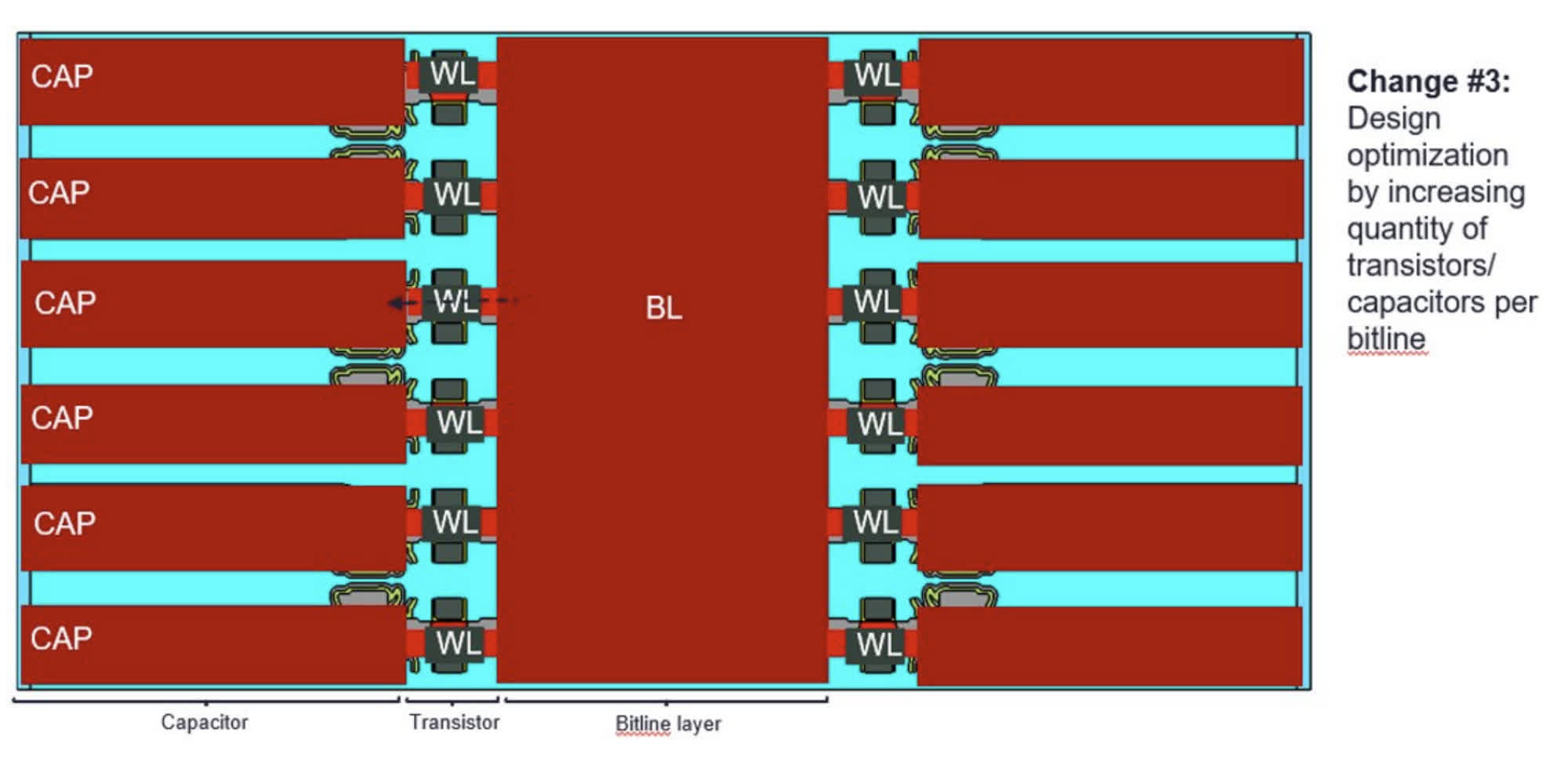
They also used novel, state-of-the-art manufacturing techniques like gate-all-around transistor design. Finally, Lam researchers increased the number of transistors/capacitors per single bitline contact by placing transistors on both sides of said contact. The resulting, "reconfigured" nanosheet can be virtually stacked in a 3D-like DRAM structure.
The first iteration of Lam's virtual 3D DRAM includes 28 layers of memory cells, and it would need a manufacturing process that's two nodes ahead of the ones used today. The stacked memory cells can be connected with a through-chip via array, which has already been done with NAND Flash memory chips.
An alternative, NAND-like approach to make 3D DRAM chips was recently proposed by NEO Semiconductor, which described its 3D X-DRAM invention as a cheap and scalable solution.